Introduction

Software Defined Radios (SDRs) are radios that are easily reconfigurable through software, thus replacing many radio hardware features. For my Hardware Design and Communications course (ECE295), teams of three students were to design one of four subsystems for the portion of a SDR that interfaces with the physical radio signal. This document outlines our design process and what I've learned along the way about hardware design and development!

The SDR was composed of the following subsystems:
  1. RX Quadrature Mixer [Subsystem A]
  2. Demodulator [Subsystem B]
  3. Local Oscillator and User/Computer Interface [Subsystem C]
  4. TX Quadrature Mixer [Subsystem D]
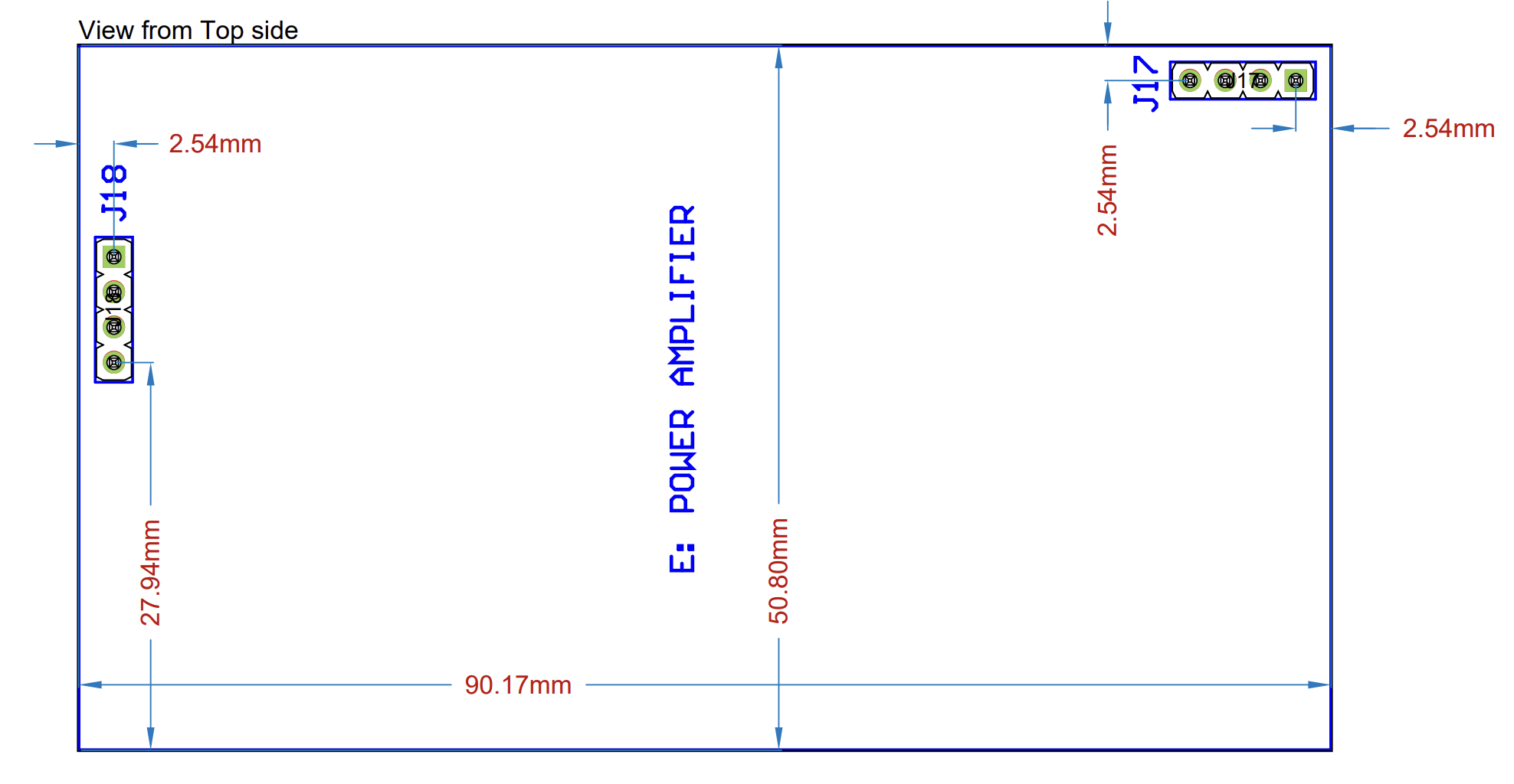
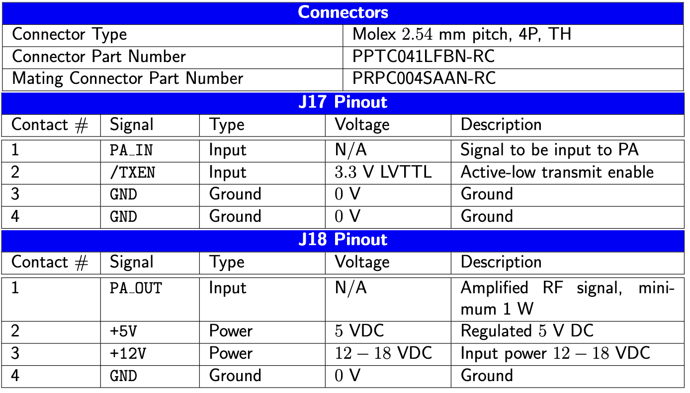
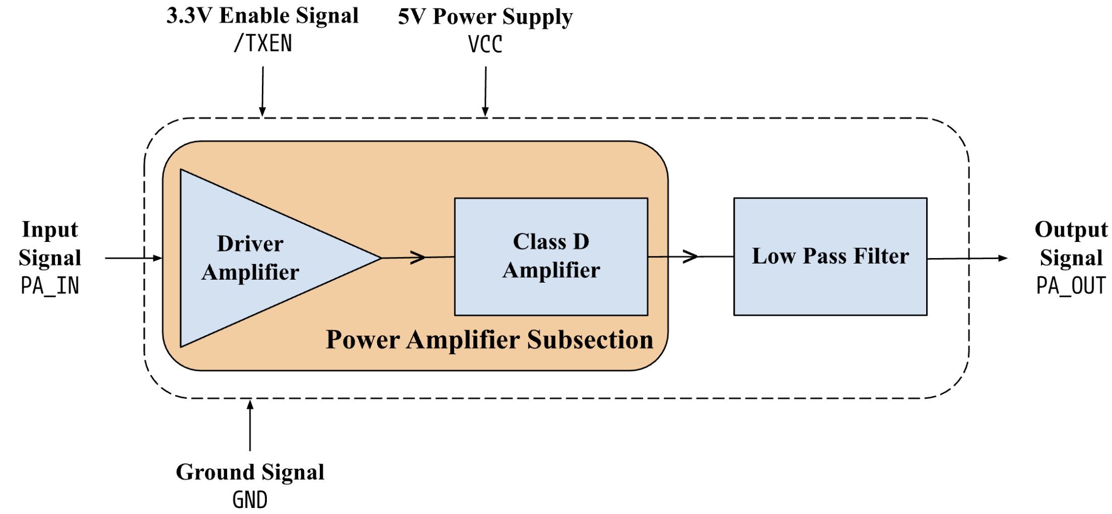
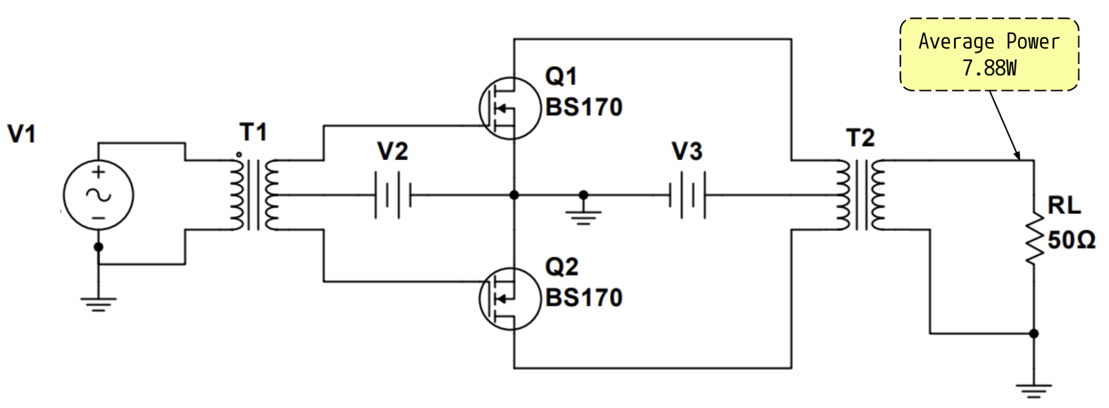
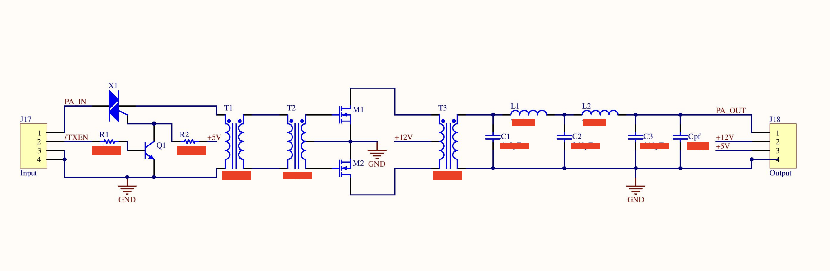
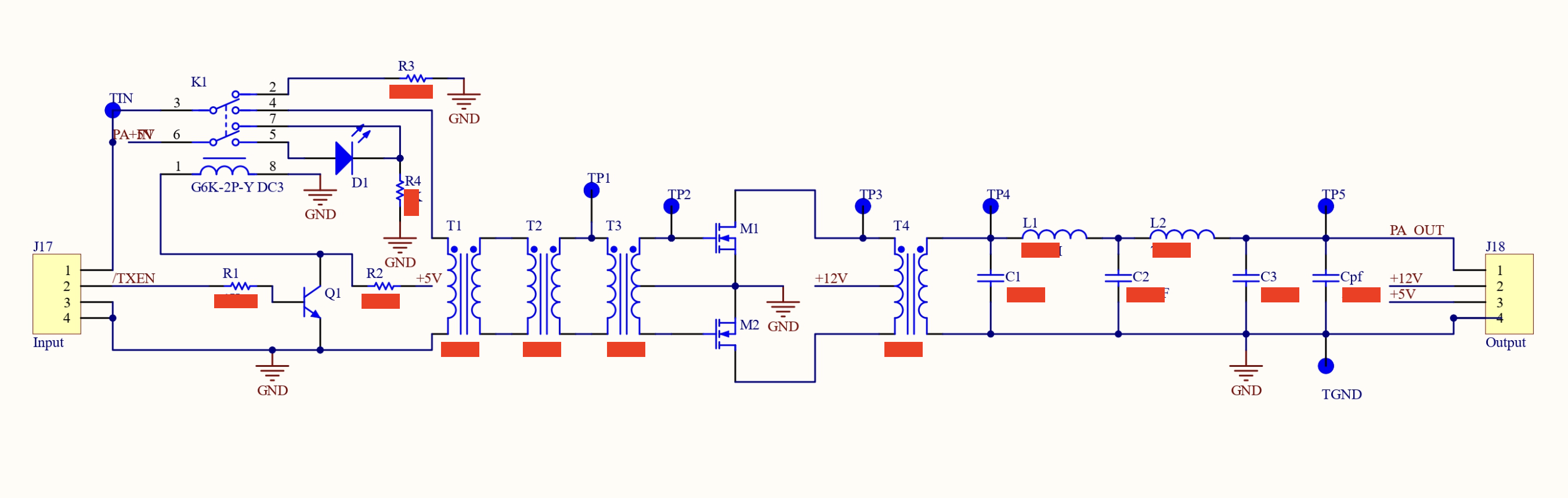
  5. X Power Amplifier and Filter [Subsystem E]

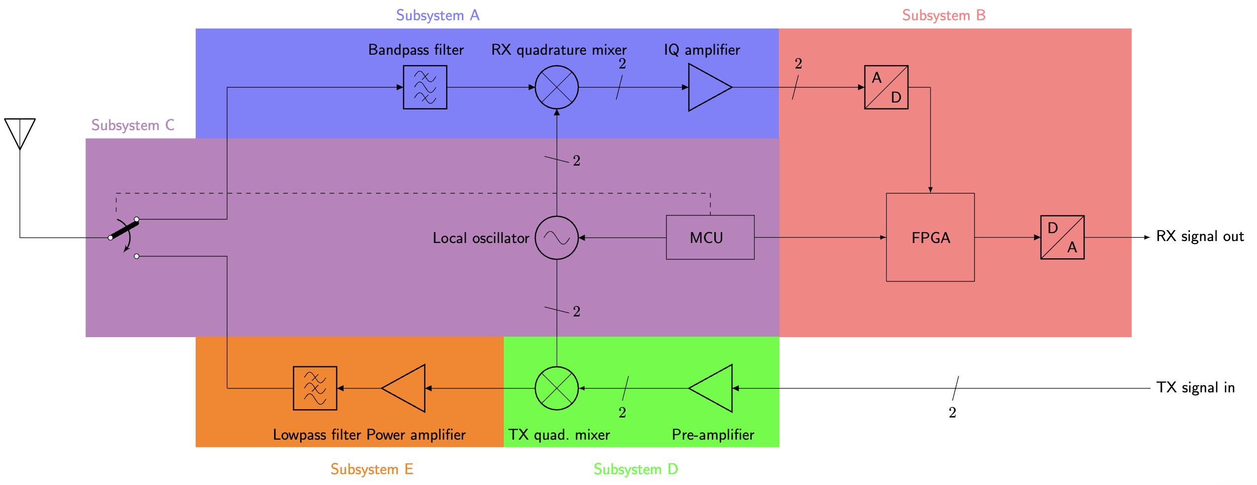
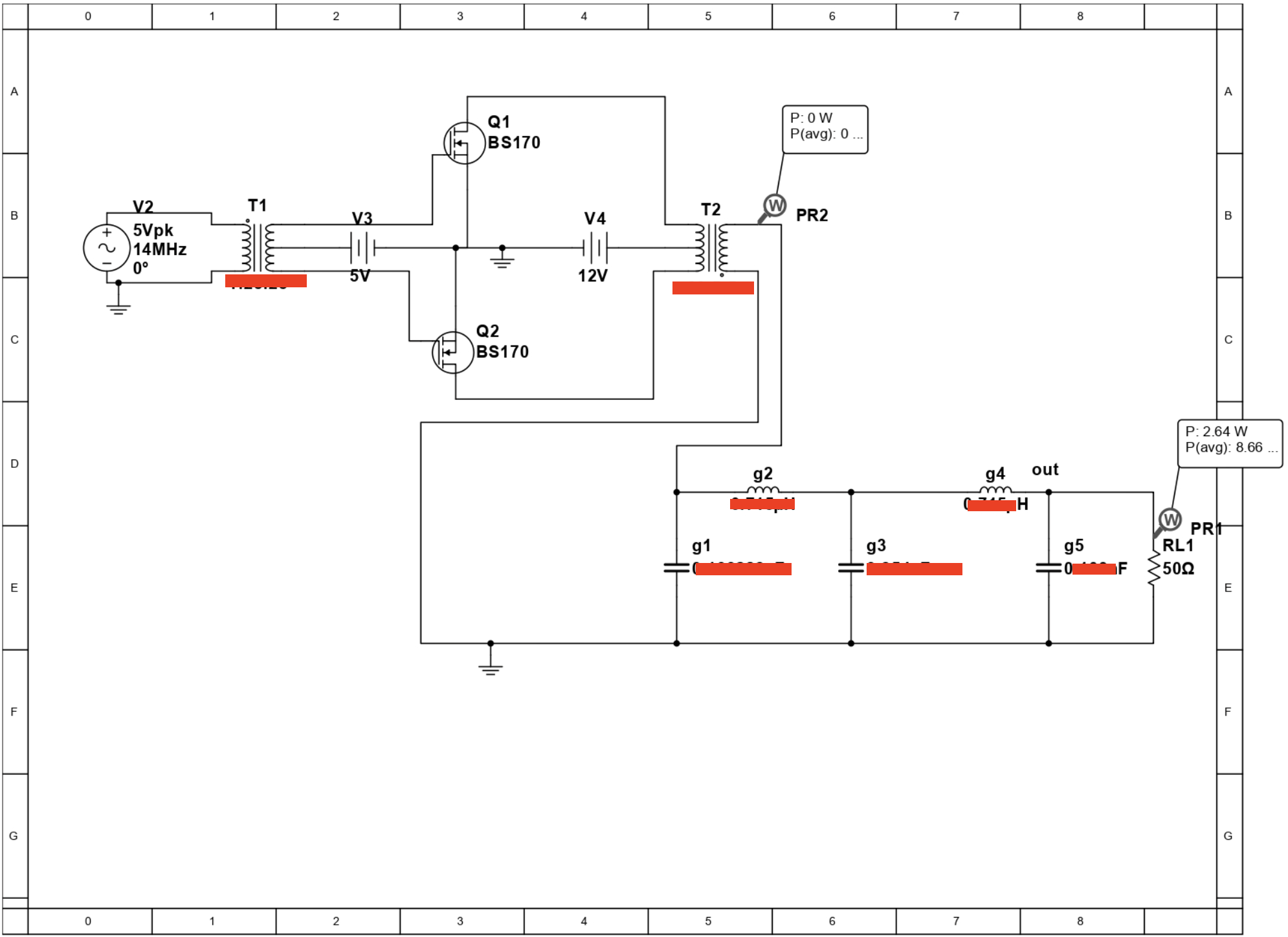
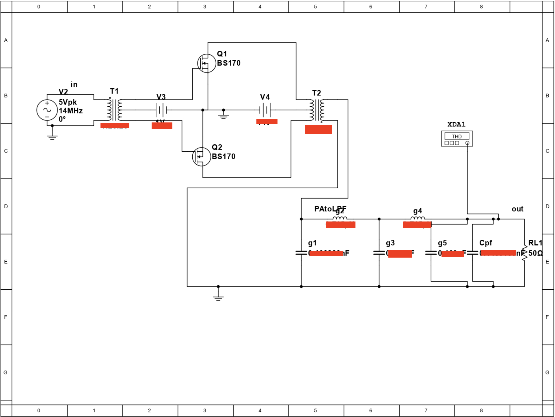
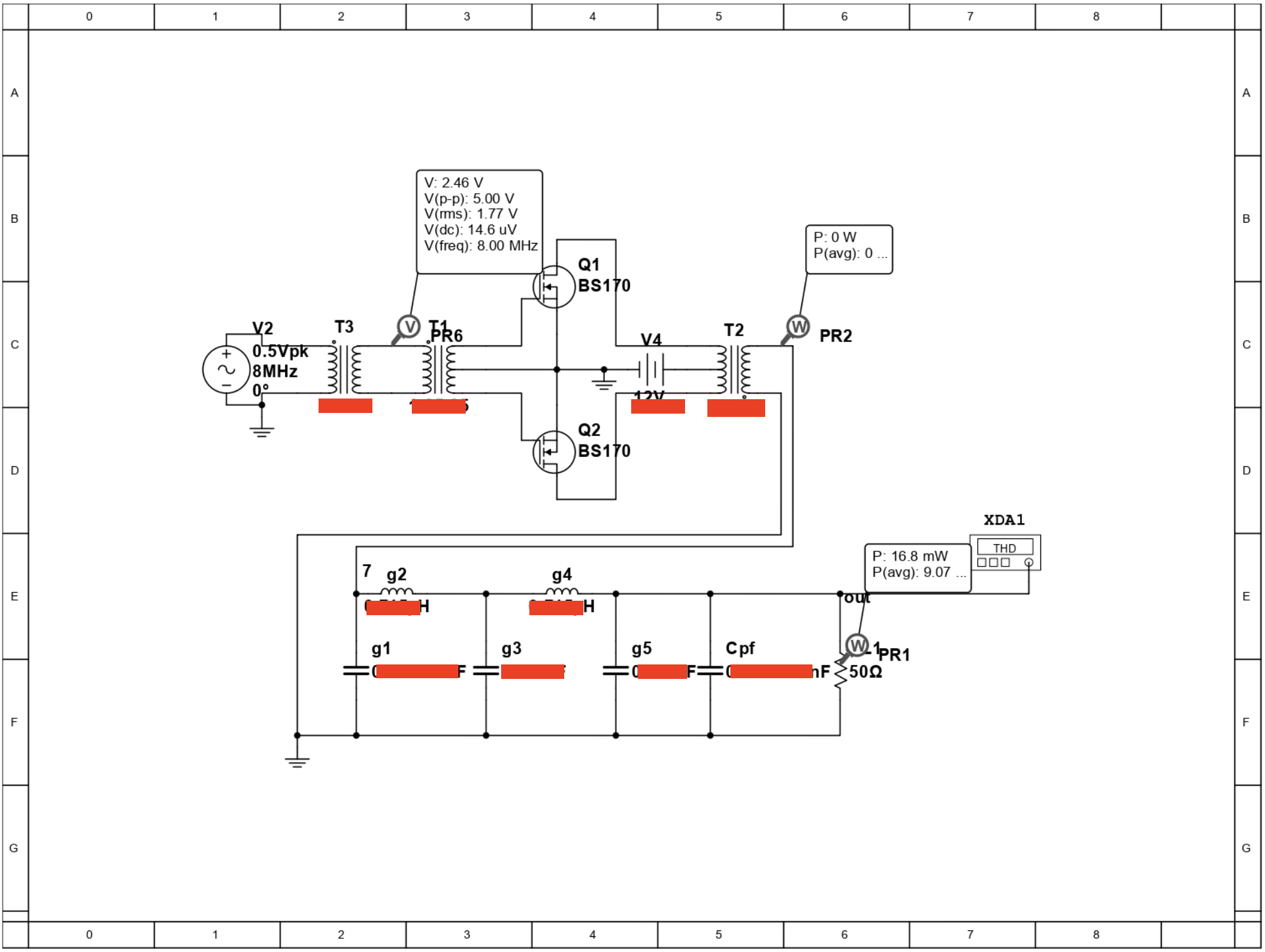
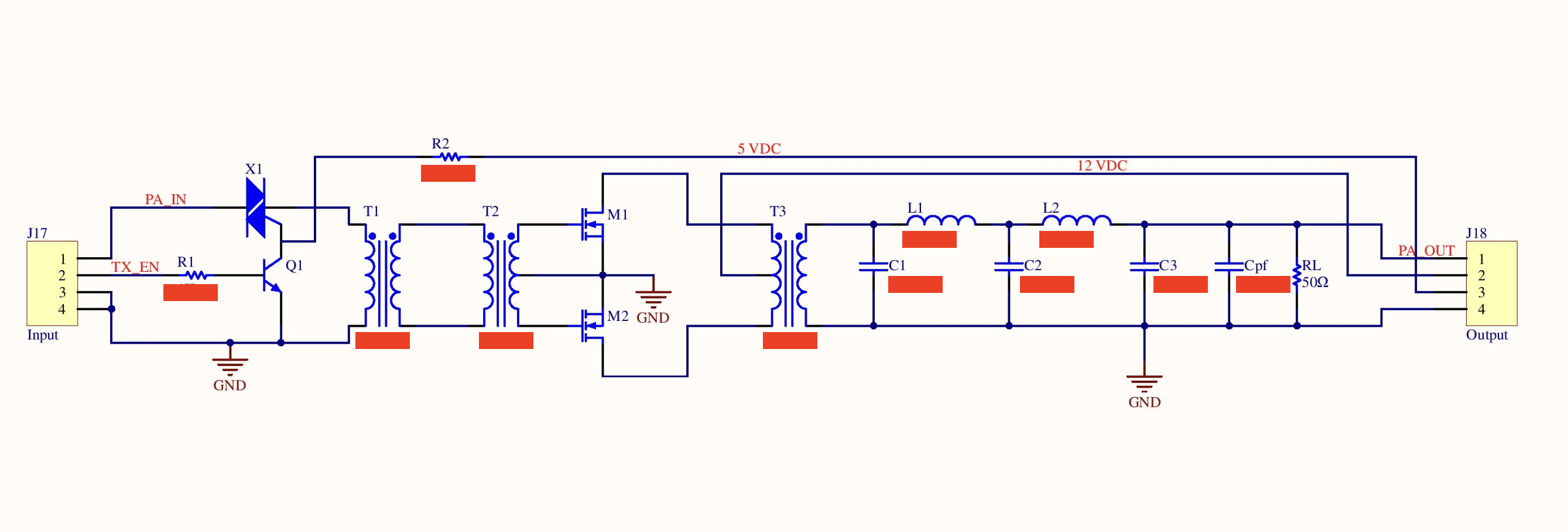
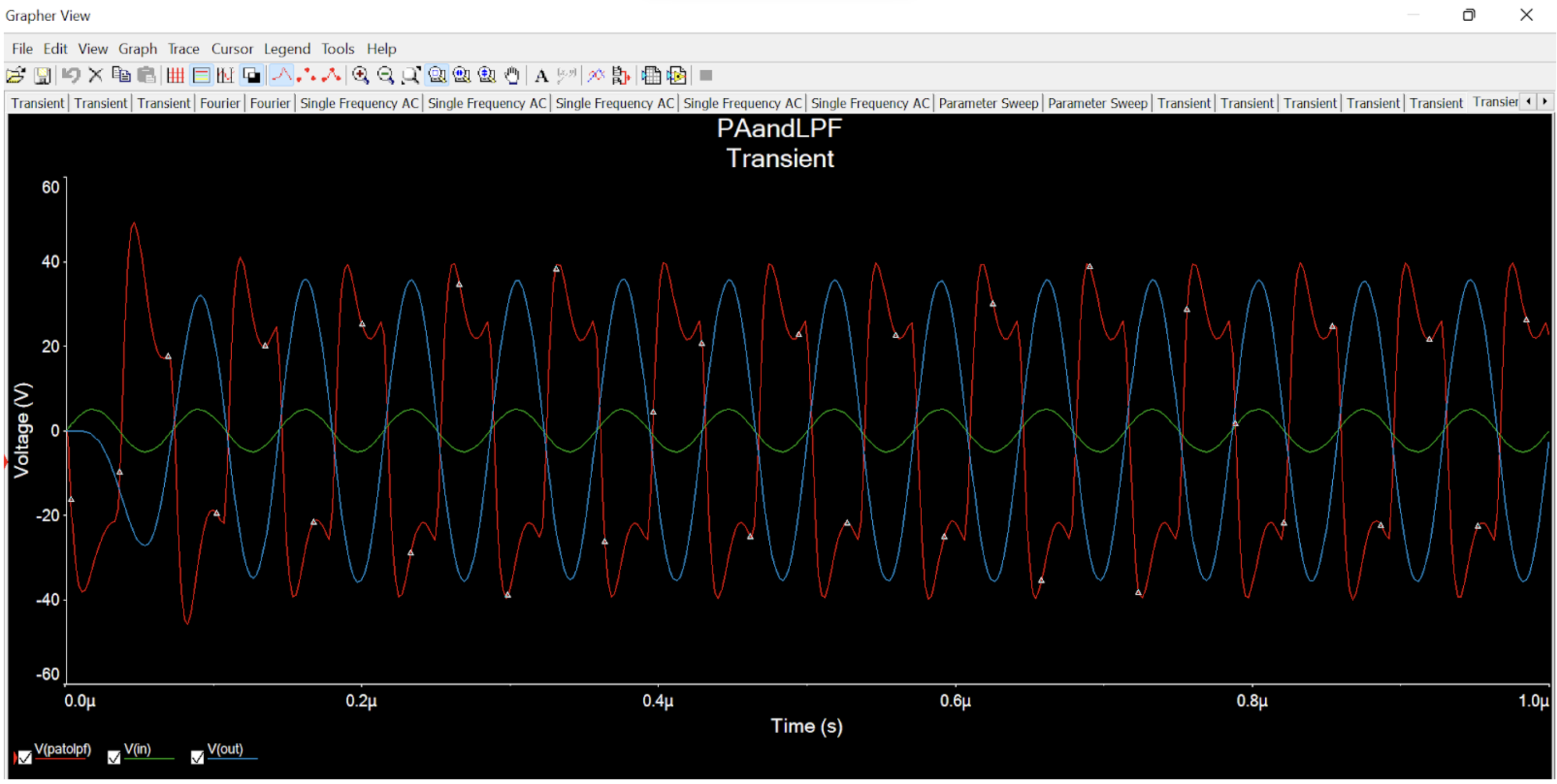
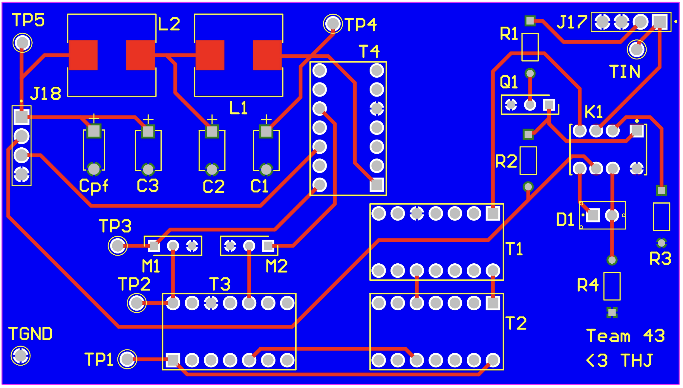
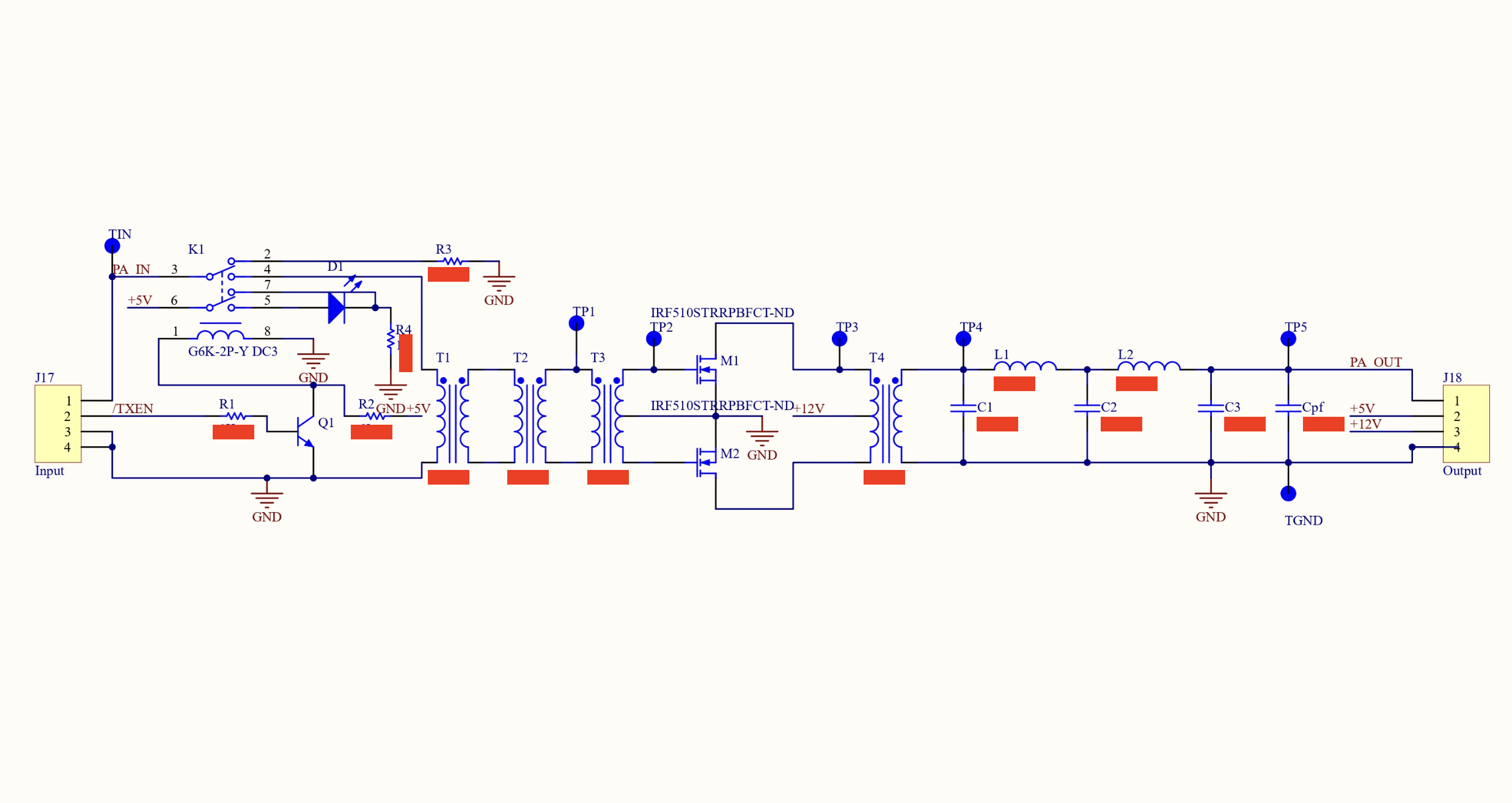
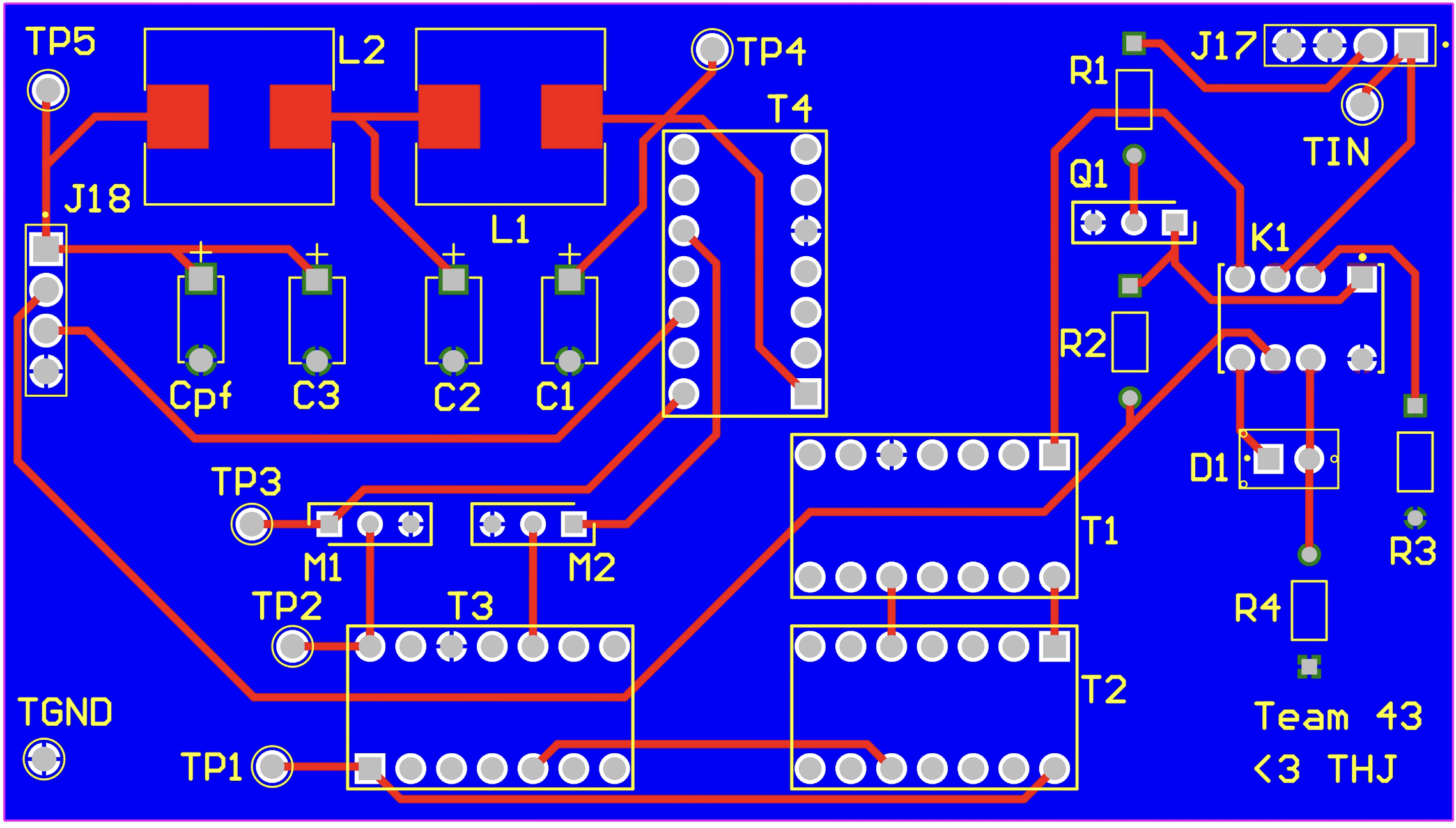
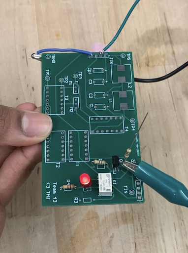
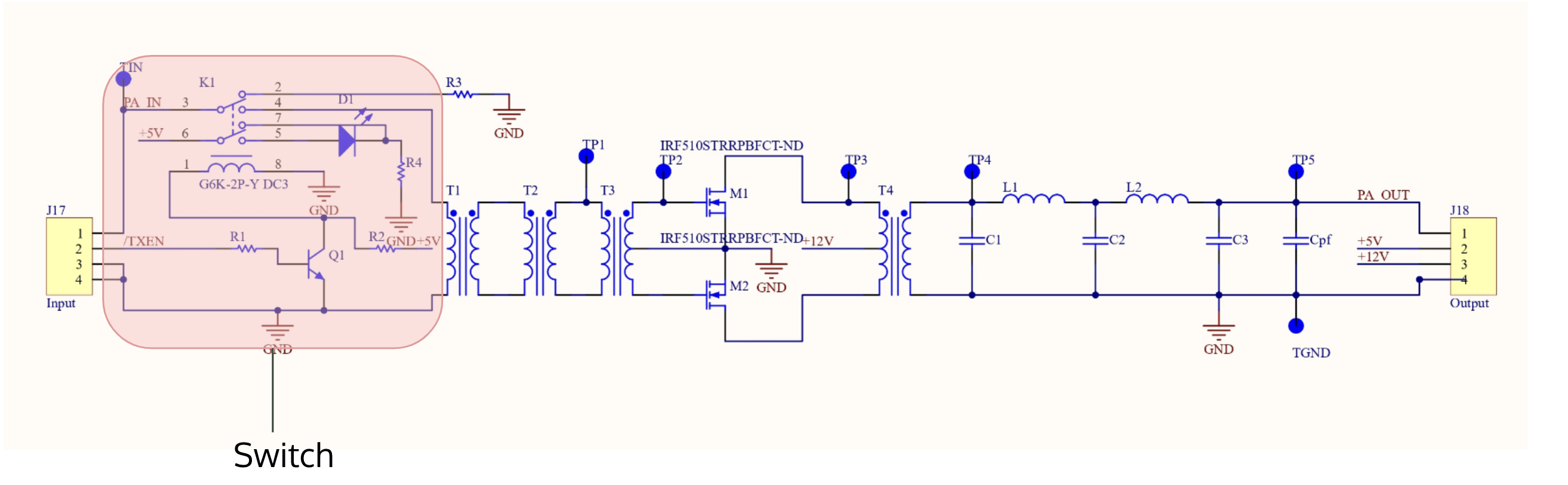
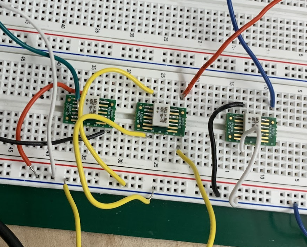
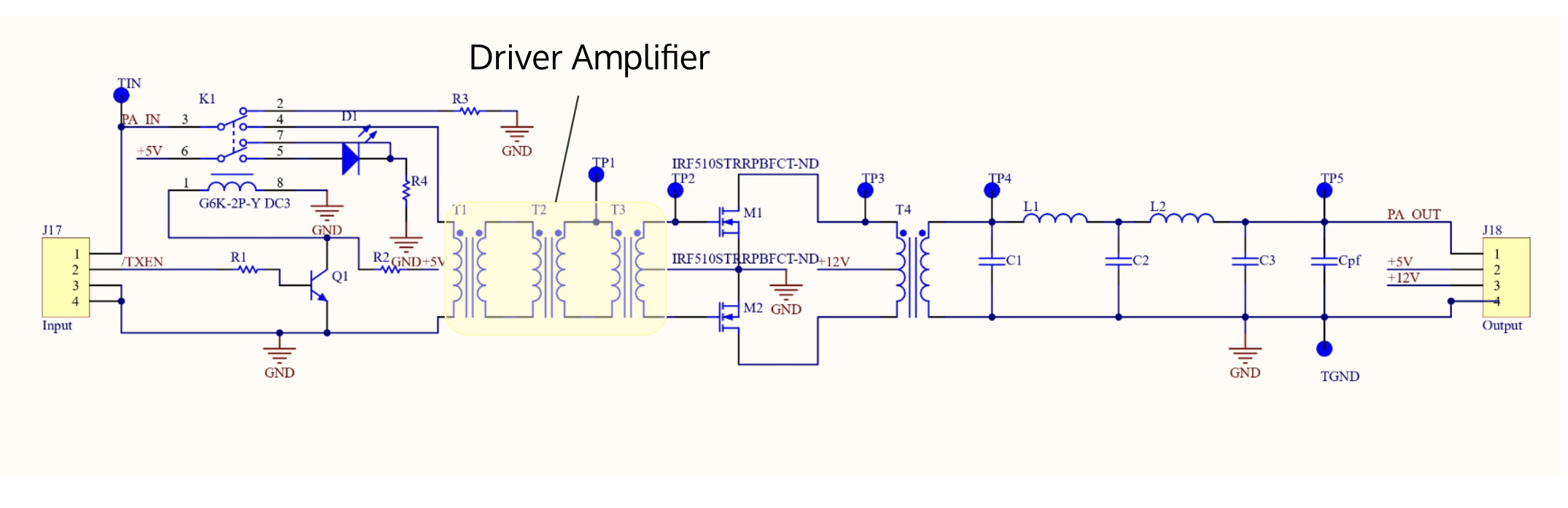
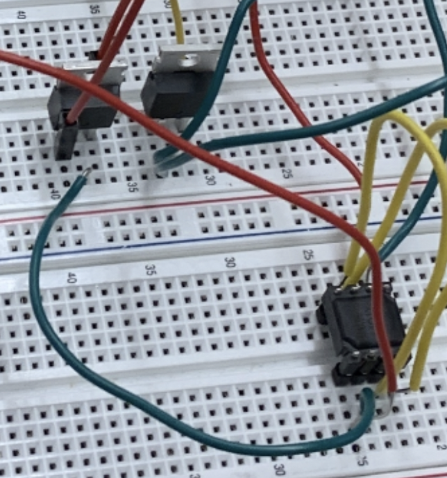
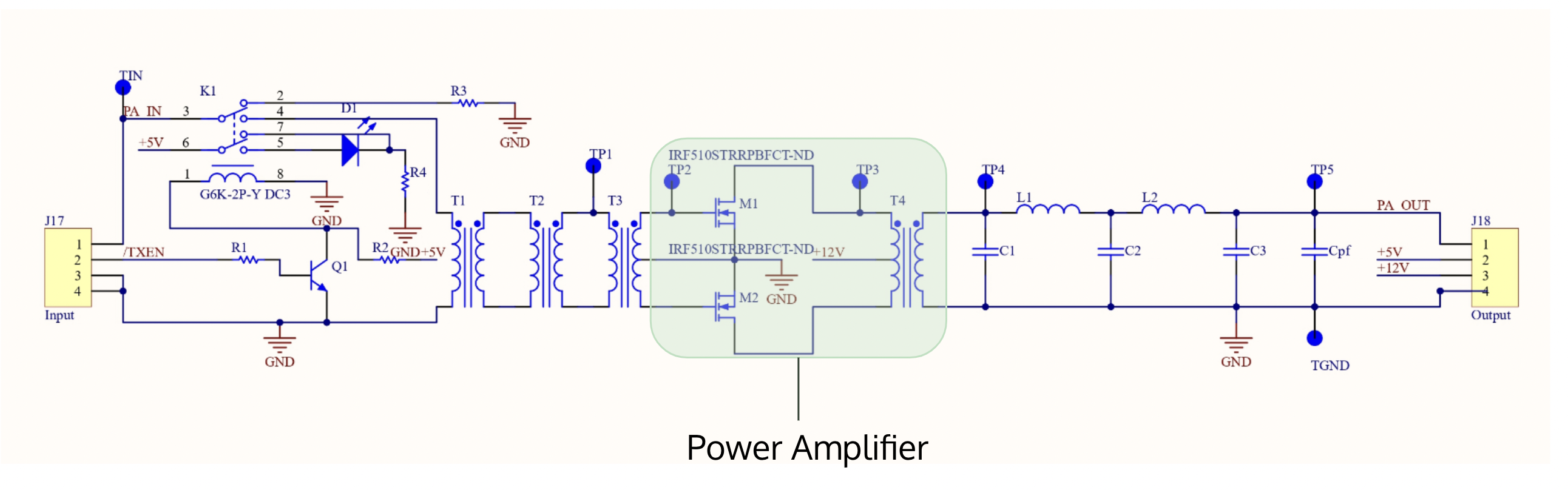
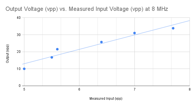
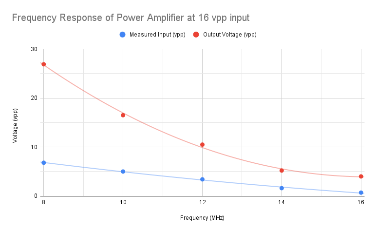
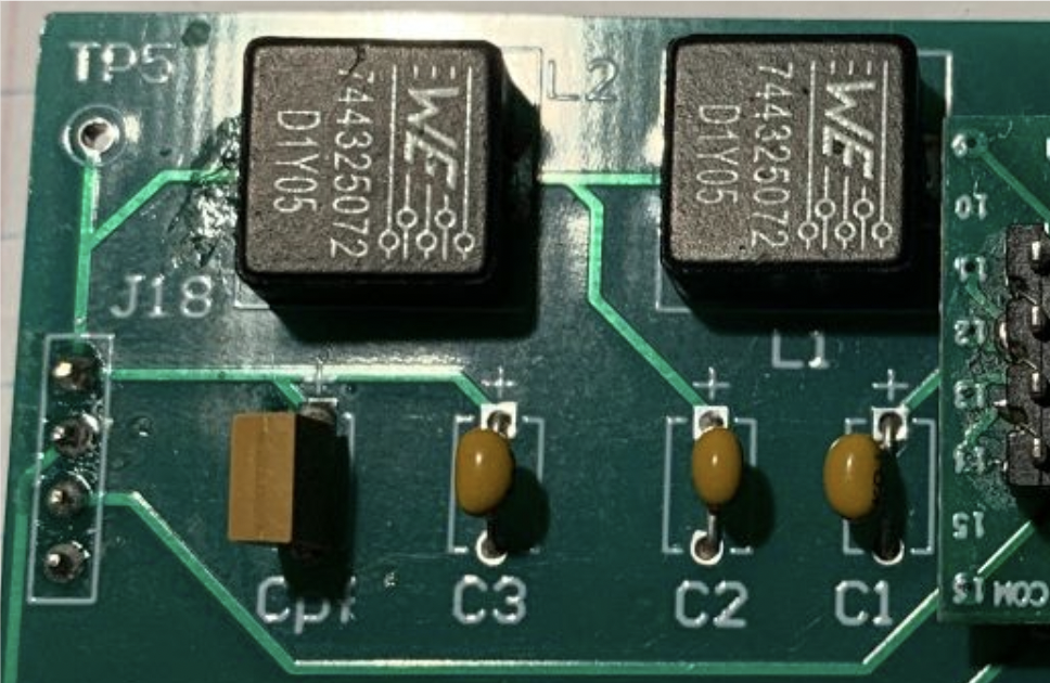
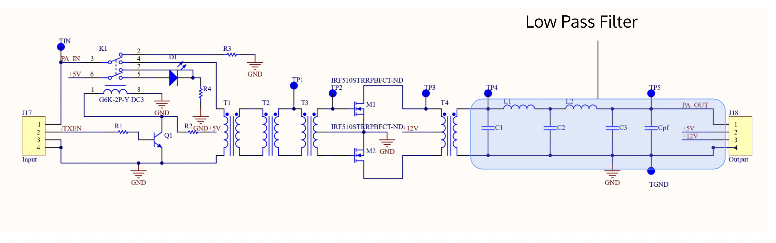
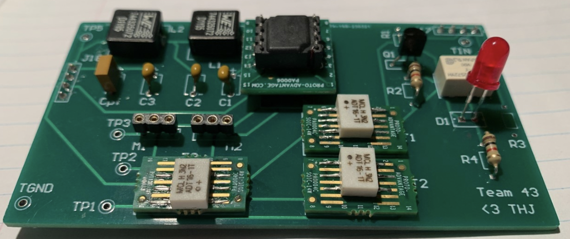
My team designed a Power Amplifier and a Low Pass filter, which is the final component in the transmitter chain. This subsystem takes the modulated signal from the mixer and amplifies it to a powerful signal that is ready to be broadcasted over long distances through the radio’s antenna. To maintain signal quality, we integrated a low pass filter to remove distortion created by the power amplifier in the process.

Our Project Management Approach:

Our team used an Agile-Waterfall hybrid approach by being flexible and iterative in the circuit design phase and more sequential in the subsequent tasks related to PCB assembly and systems integration. Over the course of the project, there were two technical design reviews, in addition to two presentations aimed at non-technical audiences. Overall, the project was structured to replicate the design cycle commonly seen in industry settings, providing students with a genuine and practical experience.

Note

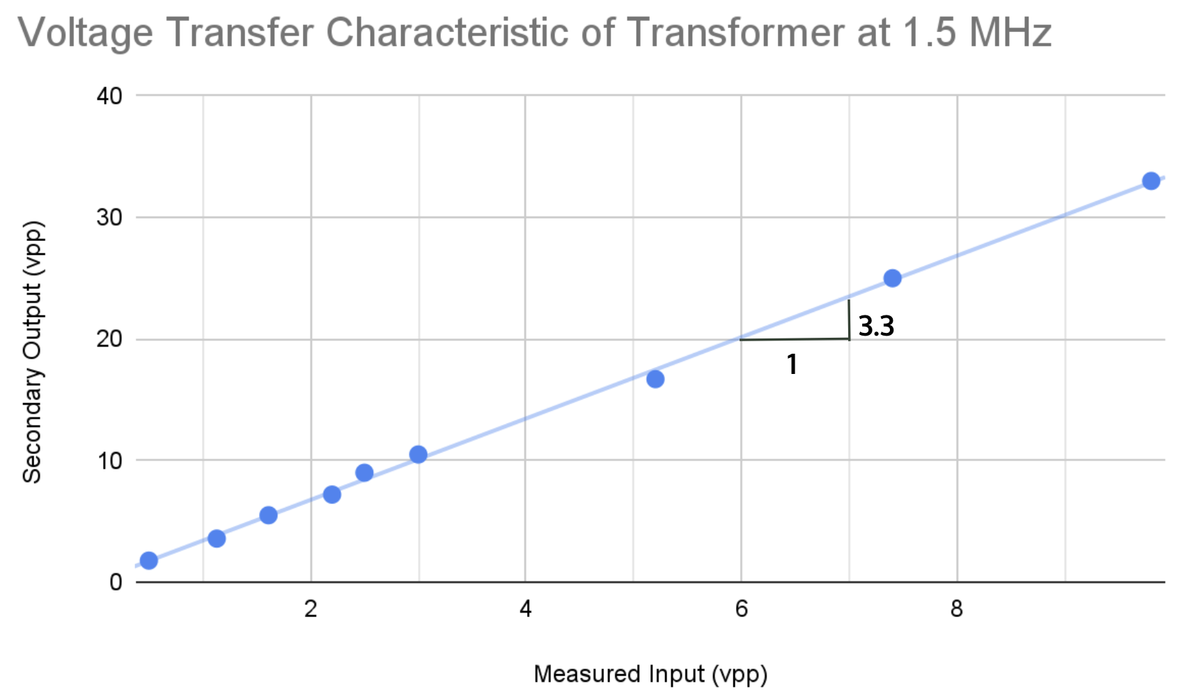
To abide by the University of Toronto's Academic Integrity policies, I will not be releasing any calculations for component values.

Design Requirements

We were provided with an interface document that outlined the electrical and mechanical connections between our subsystem and the other subsystems. This document also outlined the primary functionality of our subsystem.

Function:

The signal must be amplified to generate 1 − 10 W of continuous (CW) output power into a 50 Ω resistive load. The required total harmonic distortion (THD) is less than 10%.

Mechanical Interface Description

The Subsystem E board size must fall within 2000 mil × 3550 mil [50.8 mm × 90.2 mm]

Electical Interface Description

There are 2 connectors between Subsystem E and the mainboard: J17 and J18.

  1. Input signal 1: Modulated input signal PA IN from Subsystem D
  2. Input signal 2: active-low transmit-enable signal (/TXEN), which is at LVTTL (3.3V) levels. This signal informs the module if the radio is in receive mode (high) or transmit mode (low)
  3. Output signal 1: Amplified RF signal (PA OUT) at a level capable of driving a minimum of 1 W and a maximum of 10 W into 50 Ω resistive. Full rated power output should result when input signal 1 is full-scale]
  4. Power signals: +5V, VCC (unregulated DC)

Proposed Subsystem Design

Given that Power = Voltage x Current, a PA increases the power of the signal by generating either large voltages, currents or both at the output. PAs can be classified as either Linear or Non-Linear based on their transistor’s operating region. Linear Amplifiers (Class A, B, AB, C) produce output proportional to the input, resulting in minimal distortion but consume a lot of power. Non-Linear Amplifiers (Class D, E) produce distorted output, but are highly power efficient.

We considered this tradeoff between efficiency and linearity, and decided that the distortion can be filtered out by the low pass filter. Thus, to attain a powerful signal amplification with low distortion, our proposed design will utilize a Class D power amplifier and a Butterworth low-pass filter.

Block Diagram

I abstracted the subsystem to a black box, drew input/output arrows to/from the box, and labeled them with the signal name. It allowed to me to begin sketching out the schematic.

Target Requirements

Based on the information provided to us in the interface document, lectures and practicles, I created a set of target requirements which we could when designing our subsystem and developing testing procedures.

Requirement Target Justification
Increase transmission power 1-10W of power at the output, over a 50Ω load Very Low FM radio systems are limited to a maximum of 10 W effective radiated power [9]
Power dependent on input Output 1W of power per 0.1Vpp input signal Maximum amplification occurs when the input is 1Vpp [10]
Transmit on the TX_EN signal Output 0 W for an inactive TX_EN signal The PA should only amplify and output a signal when enable is active [10]
Filter harmonics from PA signal Frequencies higher than the 8–16 MHz should have negative dB gain Harmonics are positive integer multiples of the fundamental frequency, thus in our case will be larger than 16 MHz.
Minimize gain loss at highest operating frequency < 1dB loss at 16MHz Frequencies around the cutoff frequency experience some dB loss. 1dB is the smallest human audible change in volume [11]
Limit signal distortion Total Harmonic Distortion (THD) < 10% THD measures the distortion of the input signal. ICD allows for up to 10% THD [10]

Overall Architecture

Through Multisim simulations, we found that the following non-linear class D power amplifier generates 1 - 10W of power at the output.

The LPF design (not pictured here) will use 5 stages and a Butterworth maximally flat response. Reasons why we selected this architecture:

  • avoid the gain fluctuation of equi-ripple responses, while still ensuring a steep drop in gain near the cutoff
  • frequency response may easily be shaped by utilizing known design tables
The LPF uses inductors and capacitors because of their frequency dependent impedance. We chose an LC filter over a RC filter to avoid power loss in the resistors.

Disclaimer

This was not our final design! As be started to dive deeper into the design details, we soon found that the proposed subsystem architecture was not feasible. [link to iterations] [link to final design]

Milestone 1

Milesteon 1 (M1) marked the completion of schematic design on Altium Designer that passes the Electrical Rules Check. In this section, I will describe how we reached the milestone thorugh multiple iterations.

Revision 1.1

Combined PA and LPF

  • Power Amplifier and Low Pass Filter were integrated into a single design
  • The power across the output resistance is lower than expected
  • Input from Subsystem D is assumed to be already amplified by a driver amplifier

Revision 1.2

Power corrected LPF and PA

  • The reduction of power across the resistance was determined to be because of the reactive power generated
  • Equivalent impedance was calculated, then a Power Factor Correction (pfc) capacitor was added
  • Capacitance of the PFC capacitor was swept in a two decade range about the calculated capacitance to determine optimum value
  • Power optimized for 14 MHz

Revision 1.3

Driver amplifier added

  • The input signal is meant to be maximum 1 Vpp. Thus far, the voltage input has been assumed to be previously amplified by the driver amplifier
  • Since voltage gain is what is needed to drive the transistor into saturation easily, a transformer may be used (at the loss of current generated, which should not significantly affect the MOSFET)
  • A transformer with a turns ratio of about 10 (experimentally determined) is able to increase the voltage to the level assumed in previous designs
  • A TX_EN signal still needs to be worked into the design (perhaps with a transistor)

Revision 1.4

Adapted the schematic from multisim to Altium Designer

  • Added TX_EN (active low) functionality through usage of a TRIAC and NPN transistor
  • The TRIAC essentially acts as a signal controlled diode, and the NPN transistor acts as an inverter

Revision 1.5

Ready for M1 design review

  • Removed RL, since the resistive load is elsewhere (i.e. the antenna)
  • Added net labels in an attempt to make the schematic clearer (avoids wire crossings)
  • Footprints and supplier links added (not shown)
  • Transformer ratios were updated in order to make them feasible to wind

It works!

  • When TX_EN is low, the input signal (in green) feeds into the driver amplifier. The step-up transformer T1 amplifies the input signal PA_IN 10x to better drive the power amplifier.
  • The PA uses the center-tapped transformer T2 to step up and split the signal so transistors M1 and M2 is conducting for both positive and negative half-cycles. Another center-tapped transformer T3 combines the signals. After passing thorugh the PA, the signal is amplified (in red)
  • The LPF removes the harmonic distortion, resulting in a clean sinusoidal wave, capable of driving 9.25W over the 50 ohm load, with total harmonic distortion of below 10% (in blue)

M1 Feedback & Reflection

Linked here is the feedback we recieved from our M1 design review.

This was the first design review I have ever participated in. We had to present out design in-front of our entire class, professor, and TA. I was initially very anxious because I was afraid that our design would be rediculed by others and deemed unfeasible. However, I soon understood that deisgn reviews were meant to be criticle. They help ensure that the design meets established requirements and specifications. They serve as a proactive mechanism to catch and address issues early on in the design process, leading to better outcomes.

Milestone 2

After the M1 design review, we quickly approached the point of releasing the final a PCB design for manufacturing.Releasing for manufacturing is a big step, as this not only freezes the design but also is when real money is going to be spent. The first review foccused on, “Will this design meet the requirements?” The second review is all about questioning “Will the final PCB layout work?” Though design reviews help reduce the likelihood of mistakes, we soon found out that they won’t catch everything!

Revision 2.1

Exploring alternatives

  • One major feedback we recieved during the M1 design review was that the TRIAC was an overkill for our purposes. Thus, we explored other components (ie. relay circuit) we could use in the switch circuit to make the power amplifer active low.
  • In the pre-amplification stage, we used to a 1:10 step transformer to increase the amplitude of the voltage. However, when we were searching for component to purchase on DigiKey, we could not find a 1:10 RF transformer. Thus, we found a 1:16 (impedance ratio) centre tapped transformer, which meant that we could replace the 1:10 with two 1:4 transformers and replace the 1:3:3 centre tapped one with 1:2:2
  • Instead of using the BS170 MOSFETs we opted for the IRF510 given that the later was used for power applications like power amplifiers. It is also often used in the RF freqency which suits our purpose. This also increased output power to 8.2 W
  • To indicated that the power amplifier was activited when the TX_EN was low, we added a LED to the switch circuit.

    LED could receive large current and break our circuit

    The relay has 2 switches that can be closed using the TXEN signal, one connects input to the PA and the other connects the 5V supply to LED. This way, even if LED burns, PA still functions :)

Revision 2.2

PCB Layout

  • Decided to replace transistor footprints with DIP sockets to ensure there was enough spacing and making it easy to replace the component during assembly incase of any damage.
  • Majority of connections were able to be done on top layer with the ground plane used for bottom
  • Connector pins for J18 (+5/+12 VDC) were swapped, fixed to match version in ICD
  • Added multiple test points throughout the circuit

Final Design

Final Schematic

Final PCB

Modular design approach

Our team has taken a modular design approach, breaking down Subsystem E into four blocks: the enable signal, pre-amplifier, power amplifier, and low pass filter. This approach allows for flexibility in the design process and enables effective debugging.

Milestone 3

The foucus of M3 was evaluating the performance of the design and understanding the capabilities and limitations of the subsystem.

Assembly

Once we recieved our PCB and the components we ordered, we began soldering. Prior to conducting system-level testing, we performed peliminary testing on each module as we soldered them. This allowed us to asseses the quality of the solder joints and identify issues such as solder bridges or insufficient connections. It also enabled us to verify component orientation, ensuring that diodes and relays switches are correctly placed. We also conducted periodic continuity checks to confirm electrical connections and prevent shorts or open circuits. Through this process, I've learned that incremental testing enhances overall quality as efficient troubleshooting is facilitated when problems arise - effectively contributing to a smoother and more reliable PCB assembly.

Switch

Driver Amplifier (Pre-Amplifier)

We breadboarded the driver amplifiers and tested if they would step-up the input signal. Per our calculations, when connected in series, the three trasformers (T1, T2, T3) should increase the peak of the input signal by about 30x. However, that was not the case.

Pictured above is the relationship between the input of T1 and the output of T1. This single transformer tripples the input. So theoretically, three connectected back to back should step up the input by 27x.

When we measured 4.9vpp at the primary winding of the first transformer and 0.98vpp at the secondary winding of the third transformer. Instead of steping up the input signa, the three transformers -when connected in cascase- reduced the input signal by 98%!

What went wrong?

The decrease in amplitude can be attributed to the impedance transformation. In our driver amplifier stage, we used two transformers that have a turns ratio of 1:4. So if you feed a 1V peak to peak on the primary side, ideally it should appear as a 4V peak to peak on the secondary side. We failed to consider how the impedances in the circuit transformed from one side to the other. We set up the function generator to output a 1V peak-to-peak waveform at 8MHz connected to the primary winding of the first transformer. The secondary winding of the transformer is connected to a 50 ohm resistor for testing purposes. Given that n = 4, a 50 ohm load on the secondary winding appears as a 3 ohm resistor in the primary winding. The function generator also has an output impedance of 50 ohms which is now in series with the 3 ohm load resistor as seen from the primary winding. We can now do a simple voltage division calculation, and now we observe that our input signal has decreased from 1V peak to peak to 0.5 Vpeak to peak. Connecting another 1:4 transformer in between the source and the load further decreases the amplitude of the input signal.

Possible fix

Initially we dismissed BJT and MOSFET amplifiers because we wanted to reduce resistive losses in our circuit. In the next iteration, we would modify the architecture of the driver stage, opting for a common emitter amplifier. The common emitter amplifier uses a transistor in the common emitter configuration, with the input signal applied to the base of the transistor, the output taken from the collector, and the emitter grounded.This circuit has a high input impedance and a low output impedance, allowing it to match well with the source and load impedances of the RF amplifier.

Given that the driver amplifier was faulty, we decided to not solder it onto the PCB at this stage of the assembly.

Power Amplifier

We used a Würth transformer as a center-tapped transformer, however, as we began assembling we noted that the PCB traces were incorrect. As a result, we resorted to breadboarding the power amplifier and connected it to the rest of the board using wires. The original design called for several transformers to both step up the voltage and to convert the signal into a pair of 180° out of phase sinusoids. As I explained in the section above, the transformers in cascade did not properly amplify the signal. To emulate the effect of the transformers, two identical sinusoids 180° out of phase were generated at the same frequency and amplitude. The signals were then fed into the power amplifier.

The graph on the left illustrates that the power amplifier amplifies the input signal by about 8.44 times at 8MHz. However, the power amplifier should amplify at all frequencies between 8-16MHz. The graph on the left illustrates that at higher frequences, the amplifier deteriorates.

What went wrong?

Unexpected behavior at high frequencies can be attributed to parasitic capacitance in the breadboard used to test our components. When two electrical conductors at different voltages are close together (like for example between the pins in a breadboard), the electric field between them causes electric charge to be stored on them; this effect is capacitance. As the frequency increases, the behavior of the capacitor changes, and it eventually acts as a short circuit. Given that we are testing at a range of 8 - 16 MHz, parasitic capacitance could have created unwanted connections between circuit elements, causing the amplifier to behave odly at high frequencies.

Possible fix

Testing on a PCB would have reduced the effects of parasitic capacitance, however, given that our transformers in the pre-amplifier stage were surface mounts, it would have been difficult to debug.

Low Pass Filter

We were not able to breadboard the Low Pass Filter module because the inductor was a surface mount inducted. Thus, we soldered the inductor and the capacitor to the PCB. In the facility where we assembled the board, there were no solder paste available at the time. As a result, we soldered the inductor using the solder wire. This resulted in us repositioning the inductor and re-soldering multiple time.

The graph on the left illustrates the we acheived a smooth roll off at a cutoff frequence of 8MHz, not 16MHz. Total harmonic distortion (THD) measurements was carried out using measurements using the FFT. This was be acquired using the Python script sub-e.py

Frequency (MHz) Power (W) THD (%)
8 0.897 56.4
12 0.217 28
16 0.028 39

What went wrong?

The inductor may have been overheated and shorted. We simulated a shorted induction and the plot above (to the right) exhibits similar behavior as the blue curve on the bode plot (to the left).

Possible fix

Solder a SMT inductor using solder paste, not solder wire :(

Testing Results

Summary of Test Results

Switch PASS
Driver Amplifier FAIL
  • Fails at high frequency
  • Issues with input voltage
  • Fails in cascade (multiple transformers)
Power Amplifier FAIL
  • Fails at high frequency
  • Issues with input voltage
Low Pass Filter FAIL
  • Fails at high frequency
  • Issues with input voltage

Our final PCB did not meet the requirements outlined in the interface document. Certain modules in our our PCB did not perform as expected. This can be attributed to a number of things, but most importantly, I feel it is a result of the disconnect between the ideal-behaviour and the real-life-behaviour of circuit componenets. In our simulations, we experimented using ideal componenets, failing to take into account things like paracitic capacitence, impedences in oscilloscope probes, incorrect PCB traces and damanged parts.

Lessons Learned

Though this was not the outcome I exected, I was able to take away so much about hardware design and development.I learned how to:

  • interpret design specifications and translate them into a design that attempts to achieve them
  • apply ideas from agile methods to hardware development
  • use computer aided design (CAD) and electronic design automation (EDA) techniques for hardware development, particularily, schematic capture and printed circuit board layout tools
  • solder
  • assemble the board with electrostatic discharge (ESD) handling guidelines in mind
  • confidently use laboratory instruments to debug circuits
  • assemble instruments and controlling software for the purpose of automated hardware testing
  • prepare oral presentations and written documents on hardware design to both technical and non-technical audiences

Thank you!

Thank you for taking the time to read this document :) If you'd like to connect with me, you can reach me at: